|
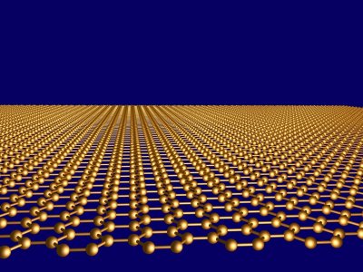
Graphene - one layer of carbon atoms arranged in a hexagonal lattice - is the newest member in the family of carbon allotropes. Although isolated graphene was reported for the first time only in 2004, the progress it made over these years is enormous, and it rightly has been dubbed "the wonder material".
There are three major areas of excitement about graphene. Firstly, it is the first example of two-dimensional atomic crystal, which very existence improves our understanding about thermodynamic stability of low-dimensional systems. Secondly, the electronic properties of graphene are very peculiar: electrons in graphene obey linear dispersion relation (just like photons), thus mimicking massless relativistic particles. And the last but not least, many properties of graphene are superior to those in all other materials, so it is very tempting to use it in a variety of applications, ranging from electronics to composite materials.
Historically, it is the electronic properties which attracted most of attention. Electrons in graphene behave like massless relativistic particles, which governs most of its electronic properties. Probably one of the most spectacular consequences of such unusual dispersion relation is the observation of half-integer Quantum Hall Effect and the absence of localisation. The later might be very important for graphene-based field effect transistors.
Generally crystals of graphene could be prepared with very few defects (consequence of ultra strong carbon-carbon bonds), which, in conjunction with the absence of localisation and high Fermi velocity ensures very high mobility of the charge carriers and short time of flight in ballistic regime. First prototypes of high-frequency transistors have been recently developed and demonstrated very encouraging characteristics.
Also peculiar are graphene's optical properties. It has been measured that graphene absorbs 2.3% of light - quite a sizable fraction for an ultimately thin material. What is even more exciting is the fact that this number is given solely by the combination of fundamental constants: πα (π=e2/hc≈1/137 is the fine structure constant). Do it at home, multiply 3.14… by 1/137 and you will get something close to 0.023.
Such combination of high conductivity (sheet resistance of doped graphene can be as low as 10 Ohm) and low light adsorption makes this material an ideal candidate for transparent conductive coating. Graphene utilisation for this type of applications has been recently demonstrated by constructing graphene-based liquid crystal and solar cells.
Furthermore, the general issue of graphene mass-production (until recently only research-size graphene samples have been available) has been resolved for these sort of applications with the introduction of a novel technique: large area thin films of micrometer-size graphene flakes can be produced by chemical exfoliation of graphite.
It is very tempting to use the unique properties of graphene for applications. The already mentioned examples do not even nearly exhaust the list of technologies which would benefit from using graphene. Composite materials and photodetectors, support for bio-objects in TEM and mode-lockers for ultrafast lasers - all those and many more areas would gain strongly from using graphene.
The issue, however, was always the mass-production of this material. Since the very first experiments, the technique of choice for graphene production for many researchers was the very naïve "Scotch-tape method", - simple peeling of graphene monolayers from bulk graphite with an adhesive tape. However, recent months seen a dramatic progress in development of truly mass-production techniques for graphene synthesis. Ranging from aforementioned chemical exfoliation to epitaxial growth (for a review see), these techniques give us a realistic hope that soon we will see products based on this exciting two-dimensional material.
1. Novoselov, K. S., Geim, A. K., Morozov, S. V., Jiang, D., Zhang, Y., Dubonos, S. V., Grigorieva, I. V. & Firsov, A. A. "Electric Field Effect in Atomically Thin Carbon Films" Science 306, 666-669 (2004).
2. Geim, A. K. & Novoselov, K. S. "The Rise of Graphene" Nature Mater. 6, 183-191 (2007).
3. Yu-Ming Lin, Keith A. Jenkins, Alberto Valdes-Garcia, Joshua P. Small, Damon B. Farmer & Phaedon Avouris, "Operation of Graphene Transistors at Gigahertz Frequencies" Nano Lett., 9 (1), 422-426 (2009).
4. R. R. Nair, P. Blake, A. N. Grigorenko, K. S. Novoselov, T. J. Booth, T. Stauber, N. M. R. Peres, & A. K. Geim "Fine Structure Constant Defines Visual Transparency of Graphene" Science 320, 1308 (2008).
5. Peter Blake, Paul D. Brimicombe, Rahul R. Nair, Tim J. Booth, Da Jiang, Fred Schedin, Leonid A. Ponomarenko, Sergey V. Morozov, Helen F. Gleeson, Ernie W. Hill, Andre K. Geim, & Kostya S. Novoselov "Graphene-Based Liquid Crystal Device" Nano Letters 8(6) 1704 - 1708 (2008).
6. X. Wang, L. Zhi, & K. Mullen, "Transparent, conductive graphene electrodes for dye-sensitized solar cells" Nano Letters 8(1), 323-327 (2008)
7. A. K. Geim "Graphene: Status and Prospects" Science 324, 1530-1534 (2009).
Copyright AZoNano.com, Dr. Kostya Novoselov (University of Manchester)
Date Added: Nov 29, 2009
|